Basic step in electronic devices construction is PCB (printed circuit board) manufacturing. Preparing PCBs at home is quite boring and long task. That made me think how to simplify this task.
I have working CNC router (as described in CNC section of this web) and I attempted to use it in PCB manufacturing process. In this article I will describe one of two procedures I finally found out. It is based on scratching paths in covering film on PCBs and subsequent etching.
Why I wasn’t satisfied with classical methods in the first place. Making hand drawn and etched PCBs is quite straightforward method. You need only resistant marker, etching liquid and of course a copper-coated board. It however requires high level of precision. I can’t even imagine drawing PCBs for packages with 0.5mm pin pitch. Soon I attempted to make some boards using photoresist coating and UV light. It is much more complicated process with many steps that can go wrong. I haven’t reached the point where I can reliable make PCBs using photoresist.
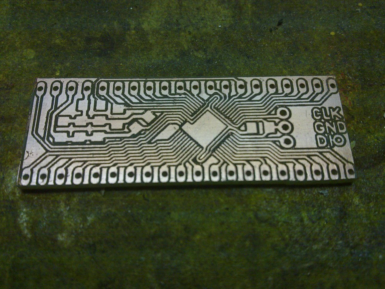
The basic idea was to get little help from my CNC router. I was bit worried about results, because my CNC was made for purpose quite different from PCB mańufacturing. At the end I discovered two possible ways. First is direct milling of the copper layer. This is fine for some basic PCBs. I will probably write some notes about this later. To get finer routes on PCB there is more suitable way – graving routes to copper covering film and then etching in classical way. I will describe this method in more detail.
CNC data preparation
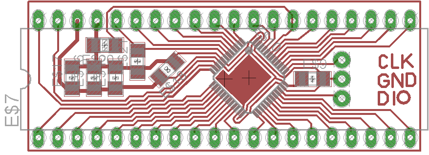
I design PCBs in Eagle software. I found plugin for direct export of CNC data – PCB-GCode. However the code generated assumes precise horizontal level of copper layer. We need to grave out only the layer of covering film so the tool position in relation to copper layer must be controlled in 0.01mm level of tolerance. That is simply impossible, just because the blank PCBs thickness varies to much.
After some thinking I found solution using simple python script. The script adds probing routines to the beginning of generated code. These routines measures the copper layer position in regular grid. According to measured data the script compensates CNC instructions and writes them to new file. Since the code is quite ugly and many parameters has to be set directly inside the code I won’t publish the code here. If you can code in Python and want to customize the code on your own, you may contact me.
CNC control software I am using (LinuxCNC) supports height probing directly. All I had to do was connecting the tool to parallel port input and to 5V voltage using pull-up resistor. Next part of the probe is the connection of GND zero potential to PCB copper layer. When the tool touches the copper layer, the input switches from 5V (caused by pull-up) to 0V of the copper layer. Software detects this transition and captures the tool height.
It took few attempts to tune parameters of the process (tool diameter, engrave depth,…). During this tunning I wasted approx. 1 square dm of raw PCB. After that I can work without any significant material loses.
Covering film
Until now I have been using ordinary permanent marker to cover paths during etching. Unfortunately recently bought markers are not enough resistant and it results in broken paths. So right now I am searching for new covering coating.
Paths engraving
I am using broken mill tool with resharpened tip to engrave paths in covering layer. It can’t be used for milling any more but is perfect for our purpose. When I run the machining program there are no other interactions required. Therefor I can attend to different activity for a while (based on PCB complexity).
Machining program begins with copper layer probing. Tool tip slightly touches the copper and in that moment machine remembers tool height. Since the contact is really brief this action won’t violate covering layer and final results. When the machine got exact PCB position, engraving phase begins. This consumes most of time in PCB manufacturing.
Drilling
When engraving is finished it is time to change tool to drill and to make some holes in PCB. Drilling instructions are part of PCB-GCode output. The drill goes through the board thickness so we can afford to drill a bit deeper and skip probing phase. When the board is removed from machine it would be impossible to set it back in exact same position. This is why the drill phase must follow right after engraving.
I recommend to fix drills in chuck as deep as possible. I usually leave only around 5 mm of protruding drill. This reduces drill tip traveling over smooth copper layer. Controlling software asks for drill replacement when necessary. The drill depth in chuck must be however approximately equal for each drill.
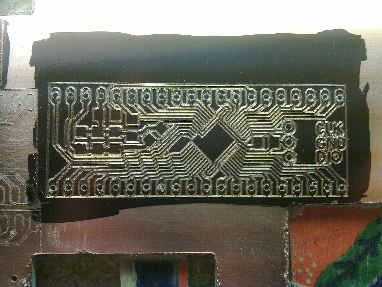
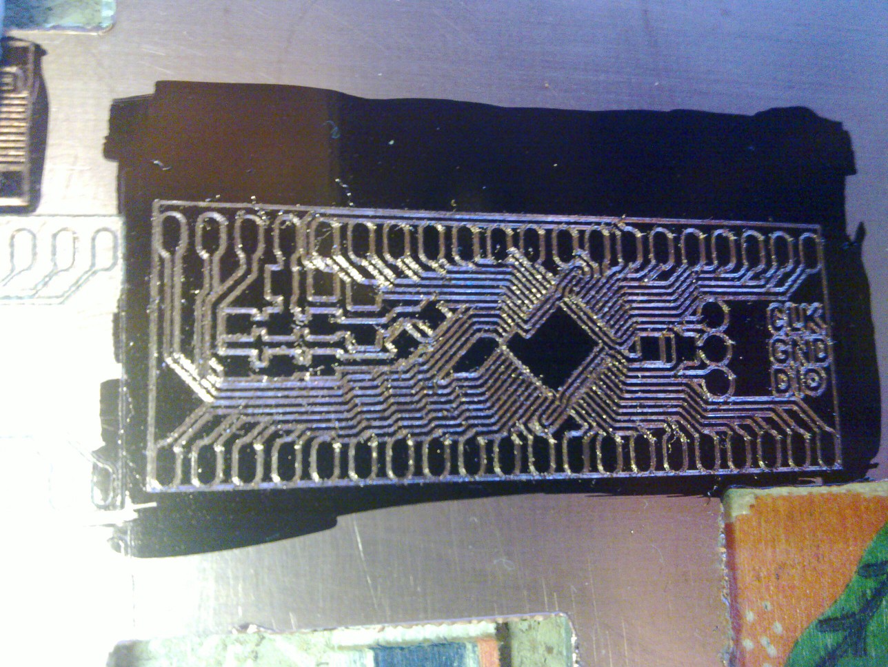
Finished PCB separation
CNC can of course be used to separate built PCB from the rest of copper board. After drilling I replace drill with mill tool and then use manual feed control to cut out the board.
Etching
Final step is same as in hand drawn PCBs or photo-resist made PCBs. I recommend to fasten isolated (!) wire around PCB to help with manipulation in etching liquid.
Results
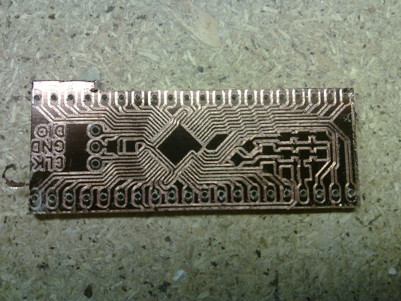
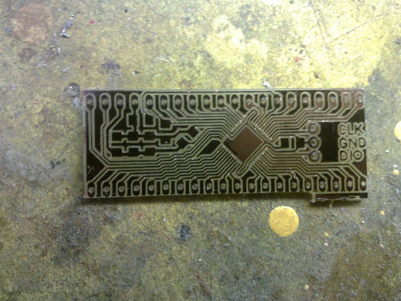
Using described procedure I am able to manufacture PCB for SMD devices with 0.5 mm pads spacing. Minimal achievable isolation width is around 0.2 mm. These values are near limit. My machine is not accurate enough to make finer motives.